
RESEARCH
RESEARCH
1.Nanomechanics
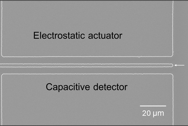
We have developed a unique tensile testing system using MEMS technology that enables direct measurement of the mechanical strength of nanomaterials inside a field-emission scanning electron microscope (SEM). Our custom MEMS devices incorporate electrostatic actuators and capacitive sensors, allowing in situ tensile tests on nanowire specimens within a modified SEM chamber.
Materials tested include carbon nanotubes, silicon nanowires, insulating nanofilms, and ultra-hard nanorods. Our work on silicon nanowires includes experimental evaluation of FIB-induced damage and the effects of vacuum annealing. Recently, we successfully measured the Young’s modulus and tensile strength of single-walled carbon nanotubes (SWCNTs) with diameters as small as 1–3 nm, establishing correlations between their structure and mechanical properties.
Materials tested include carbon nanotubes, silicon nanowires, insulating nanofilms, and ultra-hard nanorods. Our work on silicon nanowires includes experimental evaluation of FIB-induced damage and the effects of vacuum annealing. Recently, we successfully measured the Young’s modulus and tensile strength of single-walled carbon nanotubes (SWCNTs) with diameters as small as 1–3 nm, establishing correlations between their structure and mechanical properties.
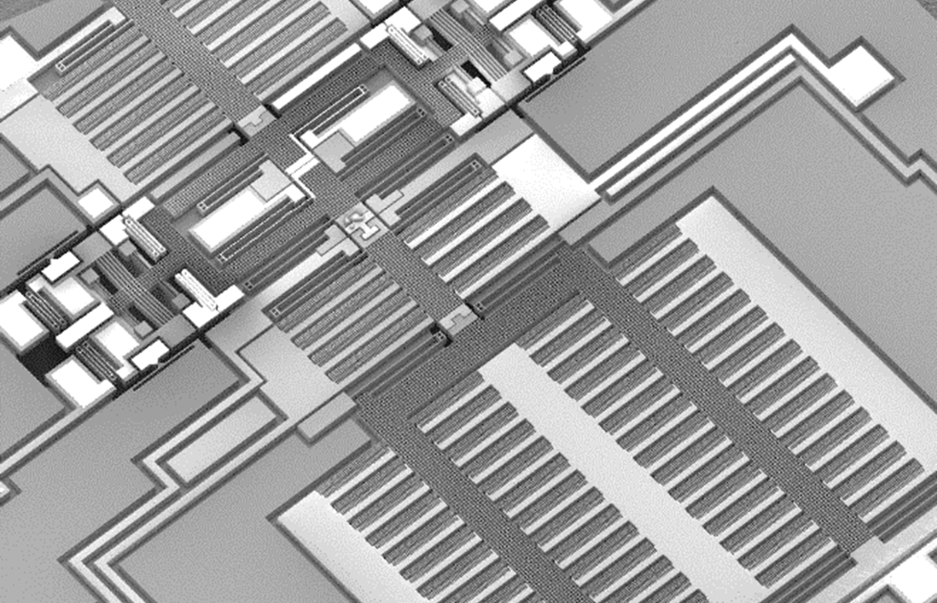
Custom MEMS device for in situ-SEM nano-tensile testing
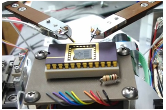
In situ-SEM Nano-Tensile Testing System

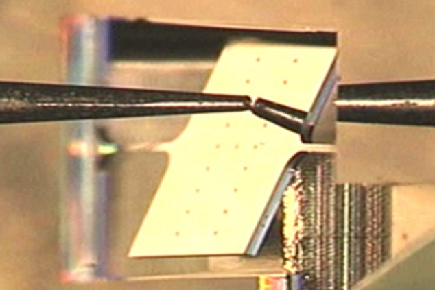
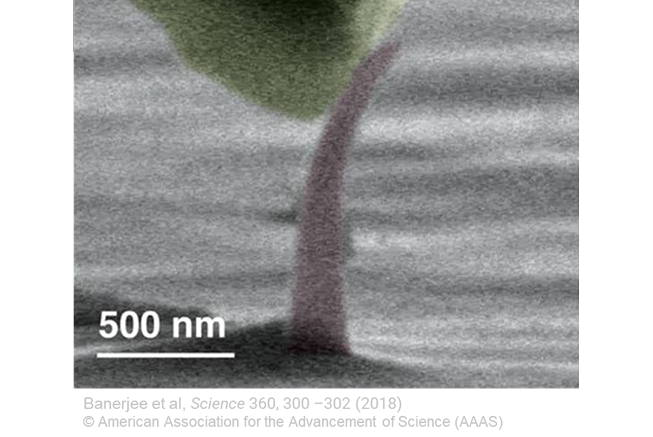
Pickup of Single-Walled Carbon Nanotube (SWCNT)

Stress-Strain Curve of a Single-Walled Carbon Nanotube
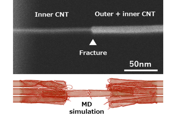
Fracture Analysis of a SWCNT Bundle

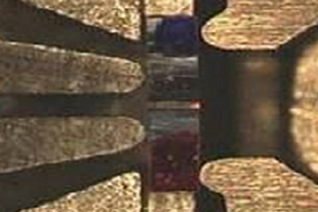
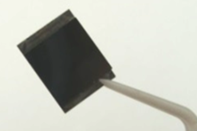
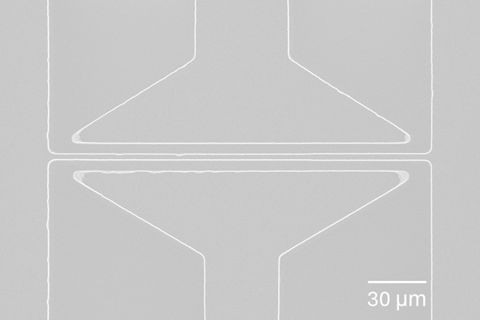
Tensile Specimen of a Silicon Nanowire (Width: 20 nm)

In situ-SEM Nano-Tensile Testing System
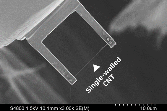
Pickup of Single-Walled Carbon Nanotube (SWCNT)
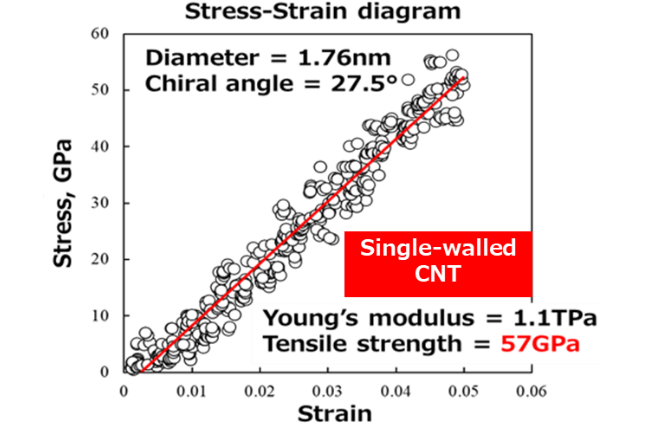
Stress-Strain Curve of a Single-Walled Carbon Nanotube

Fracture Analysis of a SWCNT Bundle
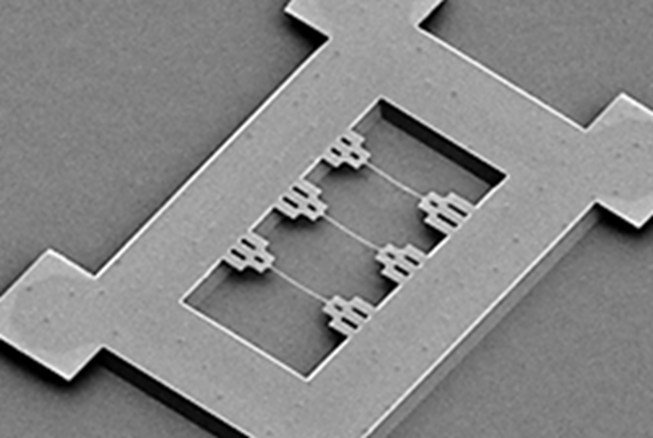
Tensile Specimen of a Silicon Nanowire (Width: 20 nm)
2.Micromechanics
We develop a variety of original experimental techniques for evaluating thin films and microstructures. These include custom-made systems for uniaxial/in-plane biaxial tensile testing, Poisson's ratio measurement, in-SEM tensile testing, and strength testing of micro rods with bonded joints. We also conduct complex mechanical testing (tension, bending, torsion) of MEMS structures and shock testing.
Materials evaluated include silicon-based films, metal films, and polymer thin films. We have measured properties such as Young’s modulus, Poisson’s ratio, fracture strength, bonding strength, creep, stress relaxation, and fatigue.
Recent studies include applying our original testing systems for stress loading on MEMS/IC devices and fatigue testing of thin films using MEMS resonators.
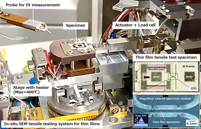
Custom In situ-SEM Tensile Testing System for Thin Films
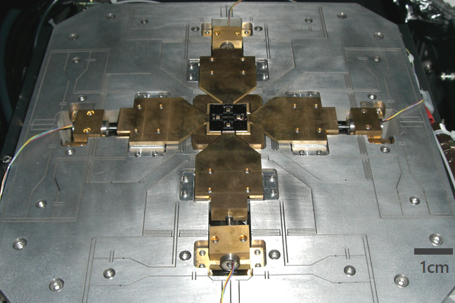
Combined Tension–Bending–Torsion Mechanical Testing of MEMS Structures

In-Plane Biaxial Tensile Testing System for Thin-Film Materials
Four-Point Bending Test of Micro-Specimens with Bonded Interfaces
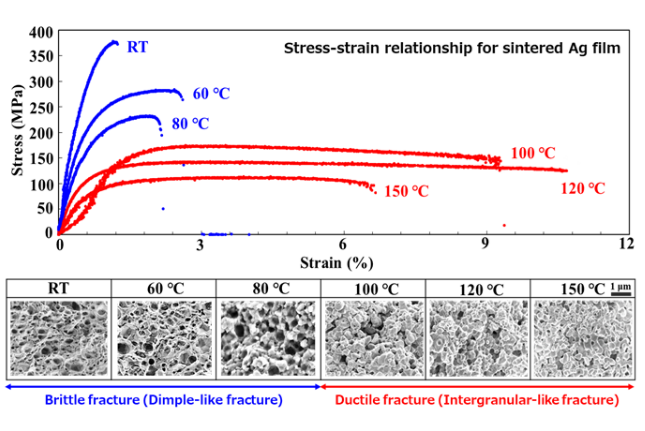
Stress–Strain Curve of Sintered Nano-Silver Film
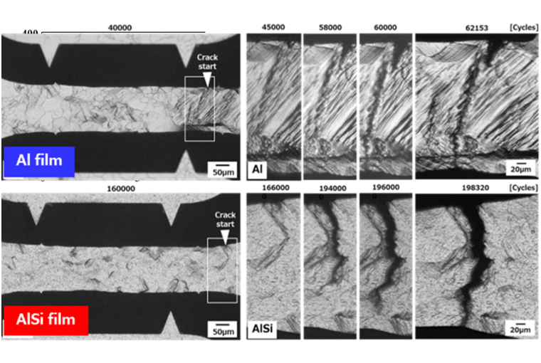
In situ-SEM Fatigue Testing of Aluminum Alloy Thin Films

Combined Tension–Bending–Torsion Mechanical Testing of MEMS Structures
In-Plane Biaxial Tensile Testing System for Thin-Film Materials

Four-Point Bending Test of Micro-Specimens with Bonded Interfaces

Stress–Strain Curve of Sintered Nano-Silver Film

In situ-SEM Fatigue Testing of Aluminum Alloy Thin Films
3.Bonding Applications of Exothermic Multilayer Films
Using our custom-designed multi-source DC/RF sputtering system, we fabricate metal multilayers composed of alternating nanolayers of dissimilar metals (e.g., aluminum and nickel). When triggered externally, these multilayers undergo self-propagating exothermic reactions due to alloying, enabling rapid and localized heating.
Such materials hold promise as compact heat sources for solder bonding and other applications. We are also developing highly sensitive multilayers that react to the slightest mechanical stimulus (e.g., a tap with tweezers), and biocompatible variants for medical and semiconductor applications.
Such materials hold promise as compact heat sources for solder bonding and other applications. We are also developing highly sensitive multilayers that react to the slightest mechanical stimulus (e.g., a tap with tweezers), and biocompatible variants for medical and semiconductor applications.
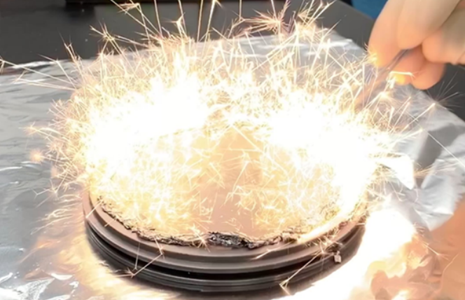
Self-Propagating Exothermic Reaction of Al/Ni Multilayer Film
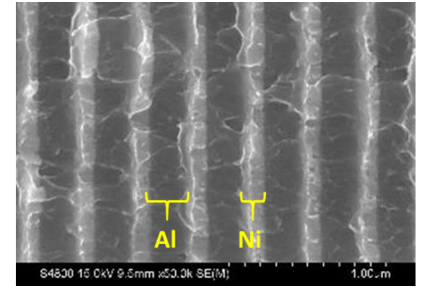
Cross-Sectional Structure of Al/Ni Reactive Multilayer Film (Bilayer: 300 nm)

Instant Bonding of Silicon Wafers
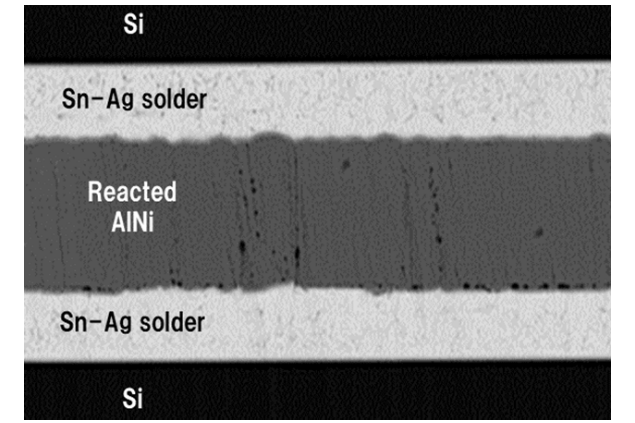
Cross-Sectional View of the Instant-Bonded Interface

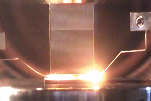
Two Silicon Chips Bonded in 0.1 Seconds

Thermal Shock Testing of Nano-Sintered Silver Heat Bonded by Al/Ni Reactive Multilayer Film

Cross-Sectional Structure of Al/Ni Reactive Multilayer Film (Bilayer: 300 nm)
Instant Bonding of Silicon Wafers

Cross-Sectional View of the Instant-Bonded Interface
Two Silicon Chips Bonded in 0.1 Seconds
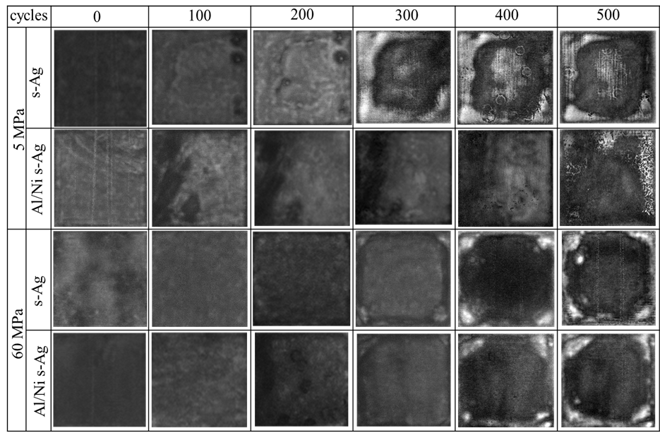
Thermal Shock Testing of Nano-Sintered Silver Heat Bonded by Al/Ni Reactive Multilayer Film
4.Functional Nanoparticles
We conduct creative mechanics research by leveraging the unique functions of nanoparticles and the physical phenomena arising from their assemblies.
For example, we have developed nanoparticles with repeating structures of biocompatible materials (e.g., titanium and silica) that exhibit controlled heating behavior. We have also created face-centered cubic (FCC) arrays of silica nanoparticles to produce structural color, enabling strain sensing through color variation.
Other projects include fabricating crystalline silicon nanodots inside silicon oxide films via electron beam irradiation to explore unconventional modulation of mechanical and electrical properties.
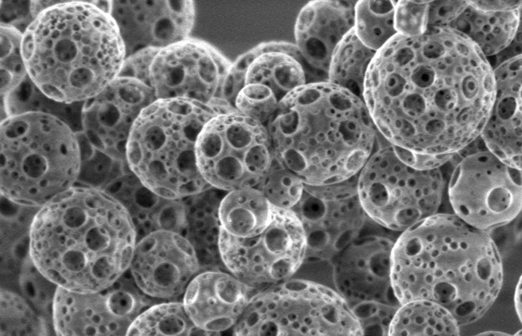
Self-Fabricated Porous Silica Nanoparticles
Heat-Generation Behavior of Ti/Silica Nanoparticles (Diameter ≈ 100 nm)
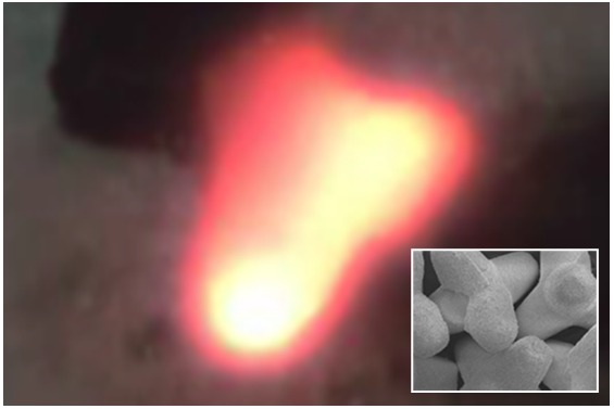
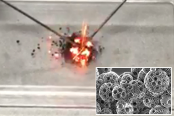
Exothermic Reaction of Al/Ni Microparticles (Diameter ≈ 500 µm)
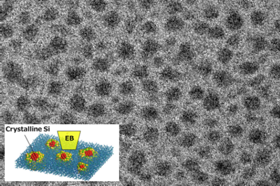
Single-Crystal Silicon Nanodots Fabricated by Electron Beam Irradiation (Diameter ≈ 10 nm)
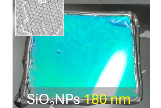
Structural Color Film Formed by Silica Nanoparticle Arrays
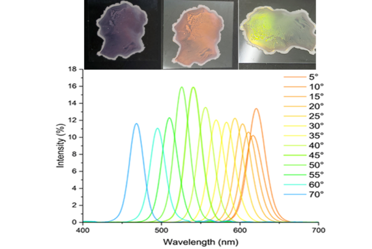
Angle Dependence of Structural Color from Silica Nanoparticle Arrays

Heat-Generation Behavior of Ti/Silica Nanoparticles (Diameter ≈ 100 nm)

Exothermic Reaction of Al/Ni Microparticles (Diameter ≈ 500 µm)

Single-Crystal Silicon Nanodots Fabricated by Electron Beam Irradiation (Diameter ≈ 10 nm)

Structural Color Film Formed by Silica Nanoparticle Arrays

Angle Dependence of Structural Color from Silica Nanoparticle Arrays
5.MEMS/NEMS Devices
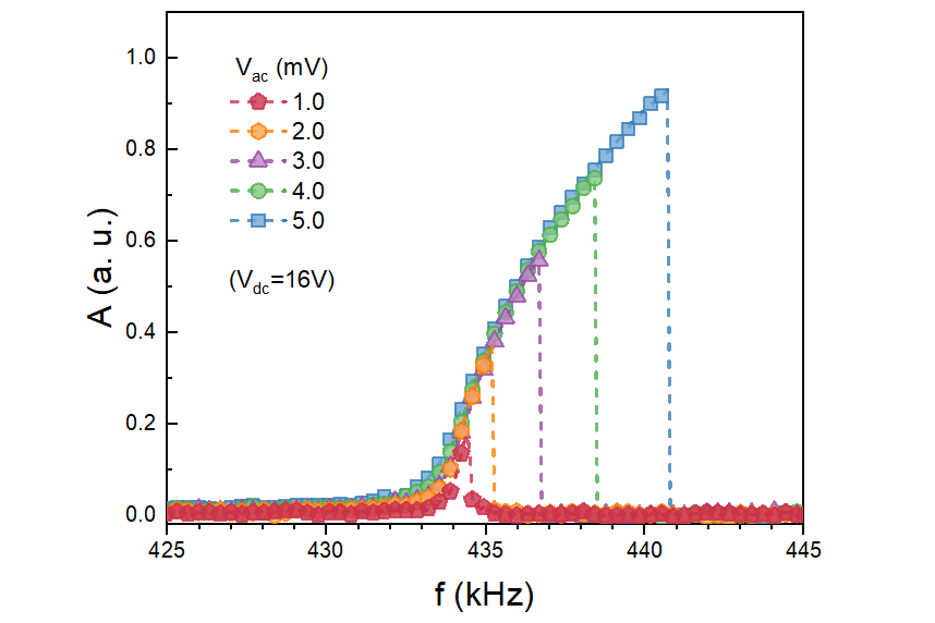
Micro/Nano Electro-Mechanical Systems (MEMS/ NEMS) are micro/nanometer-scale ‘machines’ with a multitude of applications across automotive, aviation, sensing, electronic, communications, healthcare, and AI industries. We are particularly interested in MEMS/NEMS resonator devices, where high-frequency mechanical vibration of an integrated micro/nanostructure is utilized for emerging applications in ultrasensitive sensing, efficient information processing, high-frequency signal processing, etc. The attached photograph shows an ultrathin-Si NEMS resonator device (with a width of just 20 nm) that is capable of ultrawide electrostatic tuning of resonance frequency, nonlinearity, quality factor, etc. at the application stage. We are investigating their unique dynamic properties, discovering ways to employ them for novel applications in ultrasensitive sensing and reservoir computing. Our expertise encompasses design, simulation, theoretical modelling, microfabrication, and characterization of MEMS/NEMS devices using Si, diamond, graphene, and other materials. If you are a student interested in learning about this fascinating research area, or an entrepreneur, start-up, or potential industry partner looking to consult or collaborate, or a fellow academic researcher interested in joining forces, please reach out to us.
.
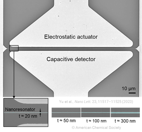
Ultra-thin, Ultra-tunable Si NEMS Resonators
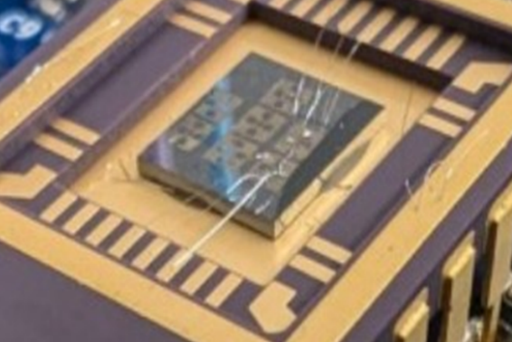
Si NEMS Resonator on Ceramic Package
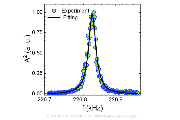
Resonance-peak Aacquired from Si Nanoresonator
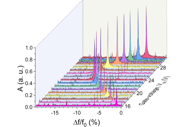
Ultra-wide Tuning of Resonance-frequency
Nonlinear-response of a NEMS Resonator
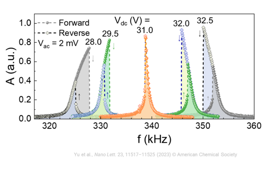
Cancellation of Cubic-nonlinearity

Si NEMS Resonator on Ceramic Package

Resonance-peak Acquired from Si Nanoresonator

Ultra-wide Tuning of Resonance-frequency

Nonlinear-response of a NEMS Resonator

Cancellation of Cubic-nonlinearity
6.Diamond Devices
Diamond is well-known as a gemstone, a symbol of eternal love and enviable wealth; it is also a very attractive material from the viewpoint of science and technology. Diamond offers a unique combination of excellent physical and chemical properties, unmatched by any other material. In addition, diamond’s excellent chemical stability and biocompatibility enable novel applications, particularly in harsh environments and healthcare. Moreover, nanoscale diamond can withstand an ultra-large elastic strain (~ 10%), which can facilitate a new class of ‘strain-engineered’ electronic devices. Thus, using diamond as a material for micro/nano-scale devices can enhance performance, reliability and extend their domain of application. However, diamond is a notoriously difficult material for micro-processing. We are investigating scalable methods for micro/nanometer-scale patterning and reactive-ion-etching of diamond for creating electronic and electromechanical devices using artificial diamond. We hope these efforts will lead to scalable fabrication and ubiquitous application of diamond devices in the future. If you are a student interested in learning about microfabrication of diamond devices, or an entrepreneur, start-up, or potential industry partner looking to consult or collaborate, or a fellow academic researcher interested in joining forces, please reach out to us.
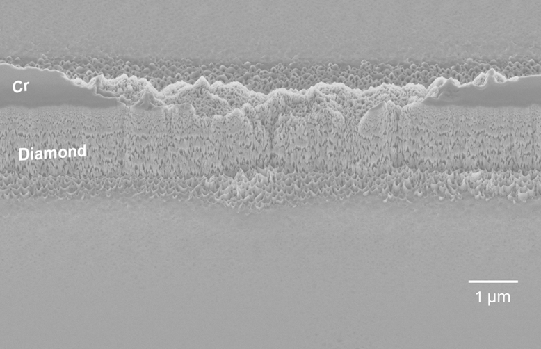
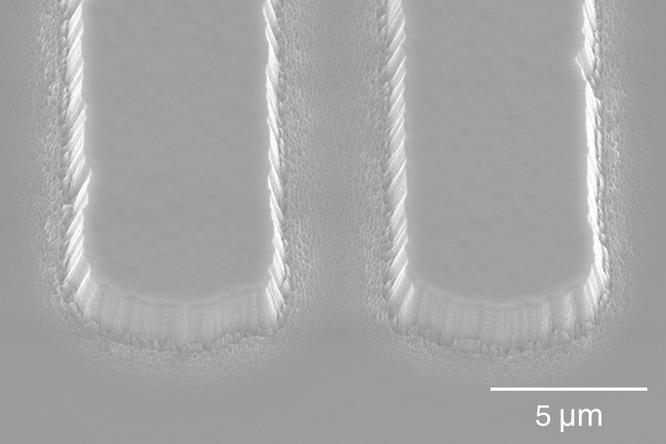
Reactive Ion Etching of CVD Diamond in Oxygen Plasma Using a Cr Mask

CVD Diamond Undergoing RIE

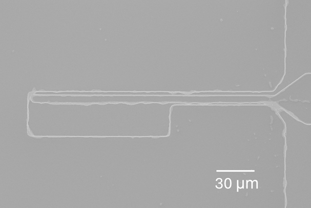
A Diamond MEMS Cantilever Device

A Diamond MEMS Resonator Device
A Diamond Thermal Actuator

Deformation of a Diamond Nanoneedle
CVD Diamond Undergoing RIE
A Diamond MEMS Cantilever Device
A Diamond MEMS Resonator Device

A Diamond Thermal Actuator
Deformation of a diamond nanoneedle